2D Tunnel FET
Reconfigurable black phosphorus TFET

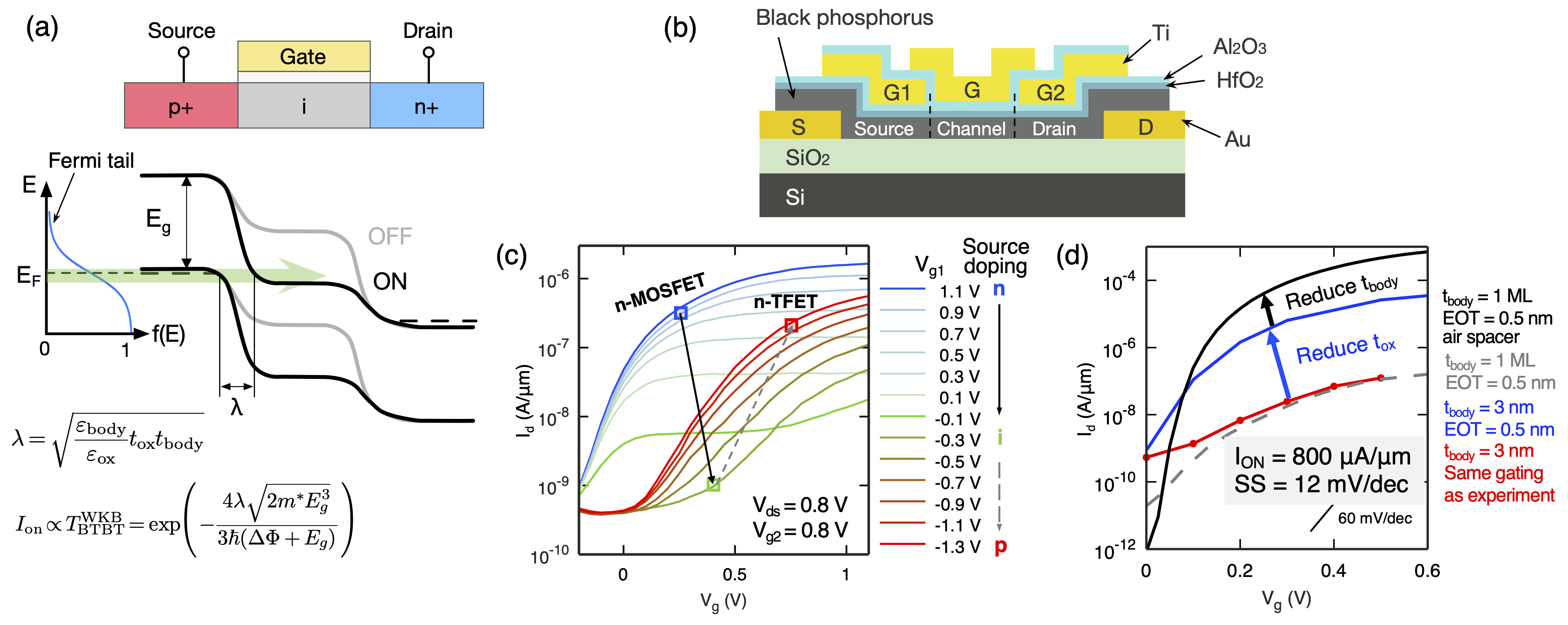
Inverse subthreshold slope (SS) of a conventional MOSFET is fundamentally to at least 60 mV/dec at room temperature as dictated by Fermi-Dirac distribution of carriers in the source. This hinders supply voltage scaling and the reduction of energy consumption. Tunnel FET (TFET) uses band-to-band tunneling (BTBT) as current injection mechanism, and the BTBT window acts as a band-pass energy filter to cut off Fermi tails and enable steep-slope switching. However, many TFETs suffer from low on-current ION due to low BTBT transmission. To boost ION, it is desired to have a small tunneling distance λ for a large BTBT probability, which requires a thin body thickness tbody. Thus, 2D materials with atomically thin body thicknesses are of interest for TFET applications (Fig. 1a).
We developed a 2D TFET (Fig. 1b) using black phosphorus (BP) as channel material, with a triple-top-gate structure that defines the doping profiles in the source, channel and drain regions. The device can also be reconfigured as a MOSFET or a TFET depending on the source doping (Fig. 1c). Although the SS of the preliminary device (~187mV/dec) is not below 60 mV/dec yet, the body thickness of BP (~3 nm) and gate oxide thickness of the preliminary device have further room for scaling. Atomistic simulation (Fig. 1d) shows that with the BP body thickness further scaled down to monolayer and the gate oxide thickness scaled down to 0.5 nm equivalent oxide thickness (EOT), SS and ION can be boosted to 12 mV/dec and 800 μA/μm, respectively.
Related publications:
-
2018
ACS NanoACS nano, 13(1), 377–385, 2018
-
2019
IEEE EDLIEEE Electron Device Letters, 40(6), 981–984, 2019
-
2017
DRCIn 2017 75th Annual Device Research Conference (DRC), 1–2, 2017