2D CMOS inverter
Complementary BP FETs and inverter demonstration

Complementary metal-oxide semiconductor (CMOS) devices have been the workhorses of the information technology (IT) industry over the last few decades. However, creating complementary n-type and p-type FETs from the same 2D channel material has been proven difficult. This lies in part in the fact that substitutional doping to create an n/p/n or p/n/n profile along the channel, as in the case of silicon devices, is hard to achieve due to the small number of atoms involved in forming the device channel. As a result, most of the prototype devices on 2D channels are using metal electrodes (instead of doped semiconductors) as source and drain contacts. The resulting devices are so-called Schottky barrier (SB) field-effect transistors, where gating includes the source and drain contact regions. Ambipolar transport is typically observed since for positive gate voltages, electrons are involved in current transport, while for negative Vg, hole transport occurs through the valence band. The goal to achieve one type of carrier injection only is thus intimately related to the question of how to suppress Schottky barrier injection of holes for an n-FET and injection of electrons for a p-FET.
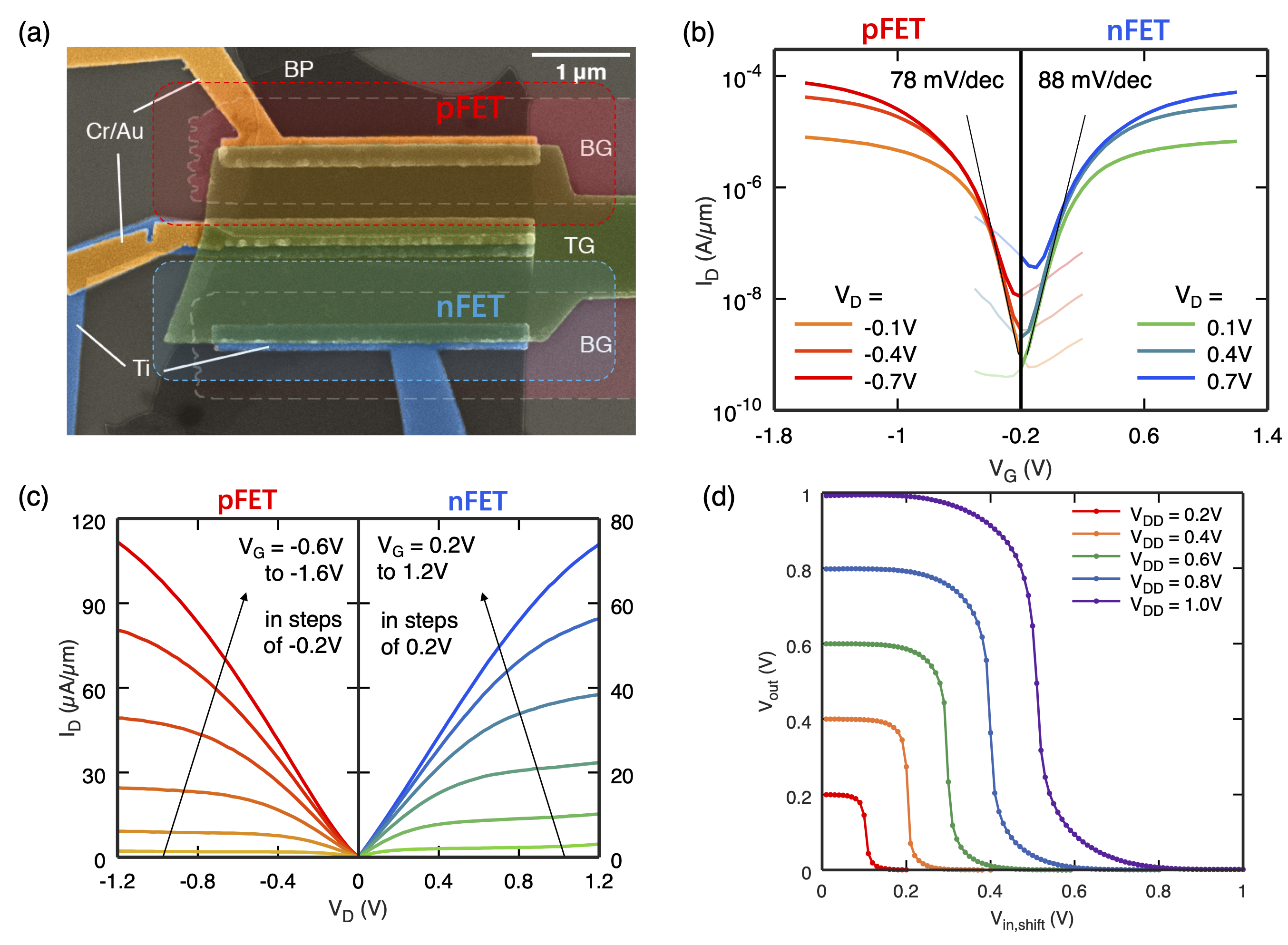
To achieve this goal, we build a device with an asymmetric double gate (ADG) on top and underneath a black phosphorus flake using source/drain metals with a preferred line-up closer to the valence band edge (p-FET) or conduction band edge (n-FET), as shown by the SEM image in Fig. 1a. By introducing the underlap of BG with respect to the drain in the ADG-FET, the impact of BG is eliminated on the drain side of the device, and thus the effective value of tunneling length λ is made larger for the drain injection than for the source injection, thus suppressing the drain injection while preserving the source injection. We have demonstrated complementary BP ADG-FETs with nearly unipolar characteristics and high ION/Ioff ratios, as shown by the transfer charcteristics in Fig. 1b and the output characteristics in Fig. 1c.
Based on the BP ADG-FETs, we demonstrate a monolithical 2D CMOS inverter (Fig. 1a). The inverter exhibit highly symmetrical voltage transfer characteristics (Fig. 1d) with large gain and remains fully operational at VDD down to 0.2V, thanks to the symmetrical characteristics of n-FET and p-FET, the output saturation behavior and steep SS in the transfer characteristics. This work highlights the potential of 2D materials for digital CMOS logic circuits.
Related publications:
-
2018
DRCIn 2018 76th Device Research Conference (DRC), 1–2, 2018
-
2019
APL Mat.APL Materials, 7(10), 100701, 2019